Global Wafer Probe Station Market Overview
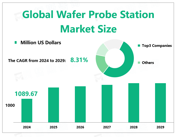
According to Global Market Monitor, the global wafer probe station market size will reach $1089.67 million in 2024 with a CAGR of 8.31% from 2024 to 2029.
Market Competition
The competition pattern of the global wafer probe market presents a high-concentration duopoly situation. Tokyo Precision and Tokyo Electronics, account for nearly half of the global market. Tokyo Precision accounted for 27.82% in 2023. It produces wafer probing machines, wafer dicing machines, electron beam lithography systems, wafer inspection systems, and chemical mechanical plagiarizers (CMP) systems.
The rest are enterprises in Taiwan and mainland China, such as Whit Technology, Wangsi Technology, Shenzhen Sidian, and so on. The localization rate of China's probe station is low, and although it has continued to innovate and catch up in technology in recent years, it still has a significant gap with international giants in terms of market share and technology. At present, the largest probe company in China is Shenzhen Silicon Power, which is gradually opening up the Taiwan market based on the mainland market.

Opportunity from the development of IoT
With the advent of the Internet of Things (IoT), more devices will connect to the Internet in the future. A large amount of data will be transmitted through the cloud, requiring semiconductor technology to transform the data into serviceable information. Semiconductor manufacturers are required to provide flexibility in test setups to accommodate a variety of designs. There is a growing need for correlation between instruments and equipment, which can only be achieved through a higher level of integration. Therefore, the requirements for accuracy will be higher and higher, and the Wafer Probe Station will also usher in new opportunities and challenges.
High performance and large range in downstream application
Wafer Probe Station has a wide range of downstream applications, not only for detecting Integrated Device Manufacturers (IDMs) and Outsourced Semiconductor Assembly and Test (OSAT) but also for academic research in electronics and materials science. Great convenience.
The semi-automatic and fully automated system uses an electric table and machine vision to automate the movement of the mold to the mold, thereby increasing the productivity of the probe station and reducing the labor required to perform multiple tests. To some extent, it saves operating costs.
Market Restraints
Thermal chucks (also known as hot chucks) are primarily used on probe systems (manual, semi-automatic, or fully automatic) to heat or cool semiconductor wafers. When integrated with the probe system, special attention needs to be paid to installing the thermal chuck. Additional cables and hoses used to heat and cool the thermal chuck create additional resistance on the wafer table, affecting movement and specifications (accuracy, repeatability, and resolution). It needs to be improved in technology to result in better test equipment.
|
By Type |
Manual |
|
Semi-automatic |
|
|
Fully Automatic |
|
|
The fully automatic segment holds the largest market share. |
|
|
By Application |
Integrated Device Manufacturers (IDMs) |
|
Outsourced Semiconductor Assembly and Test (OSAT) |
|
|
Research Institute |
|
|
The outsourced semiconductor assembly and test (OSAT) segment occupies the biggest share. |
We provide more professional and intelligent market reports to complement your business decisions.